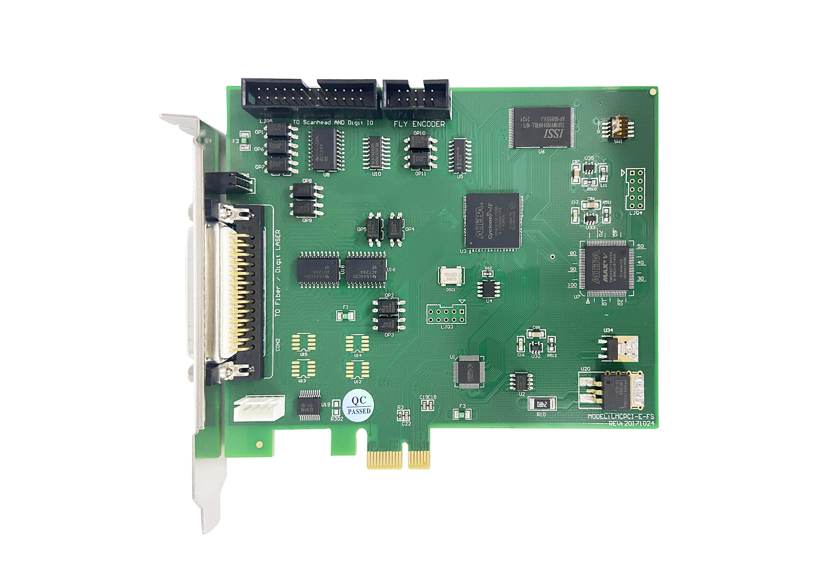
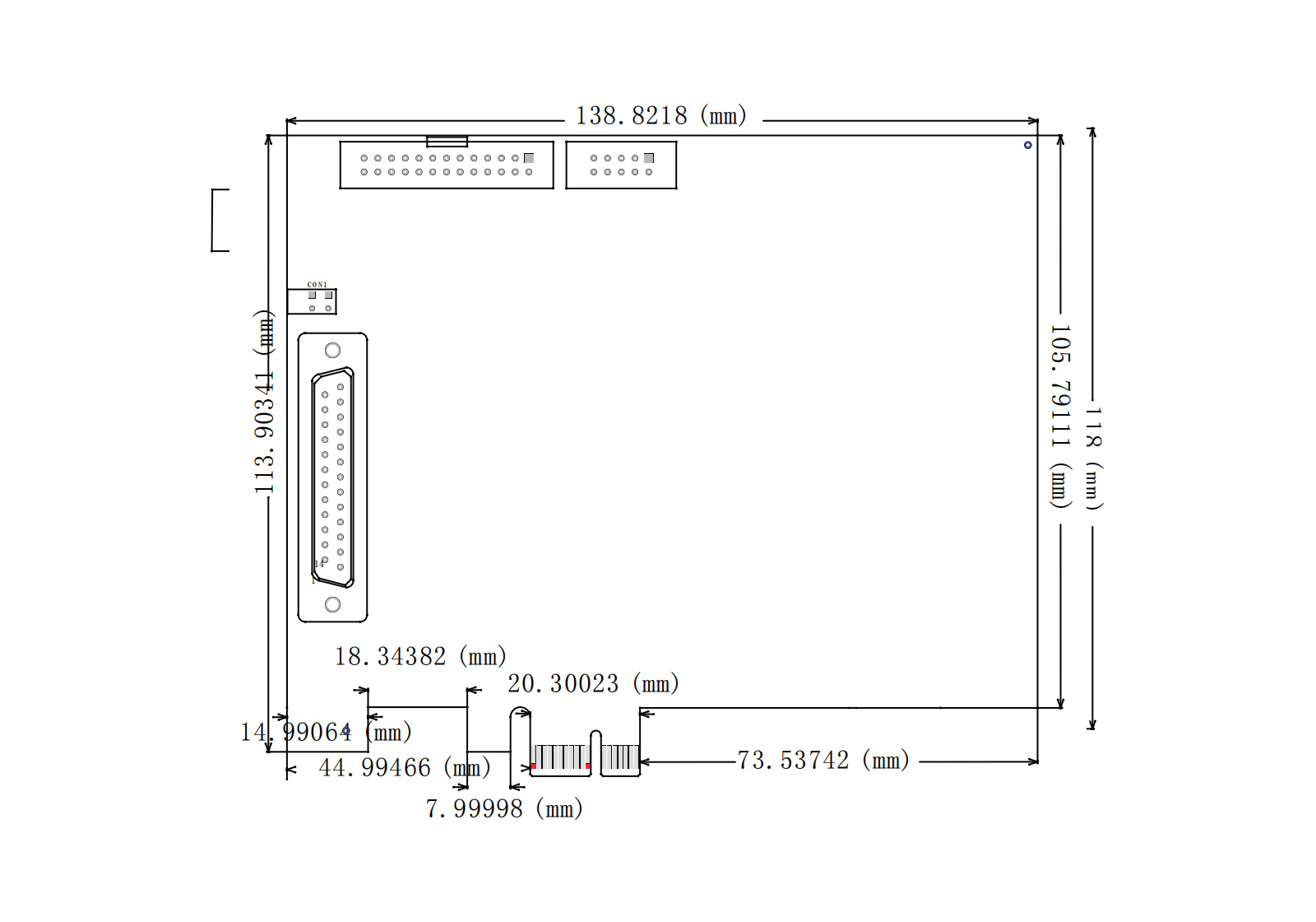
PCIE-FB
Main Configurations
- Surface:PCIE
- Input Number:6
- Output Number:2 TTL
- Operating System:XP/WIN7/WIN8/WIN10, 32/64 Bits
- Galvo Signal:Digital signal, compatible with international common digital scanners
- Compatible Lasers:Fiber lasers
- PWM Lasers(MOPA):✔
- Built-in Chip for encrytion:No need for an external dongle
- ReMark Signal:Repeated marking of cache contents
- Applicable Materials:Metal, black photosensitive materials
Applications
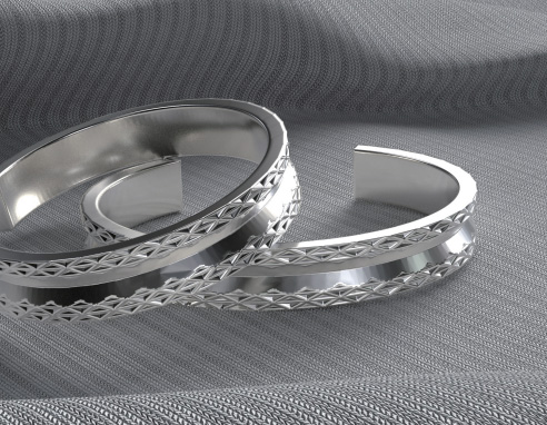
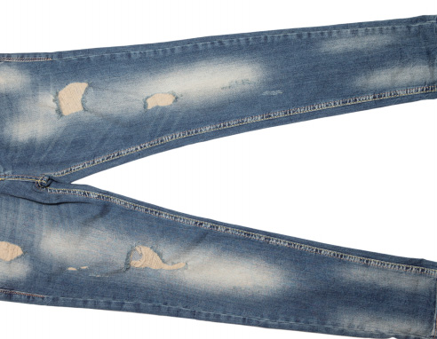
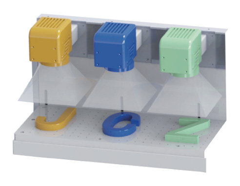
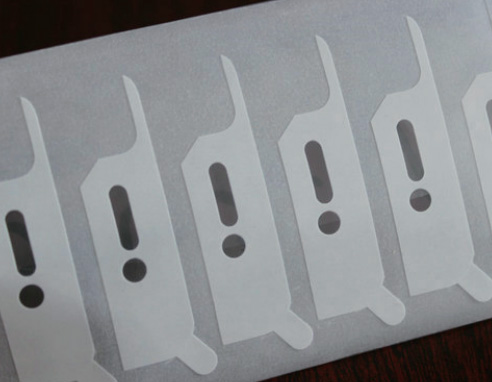
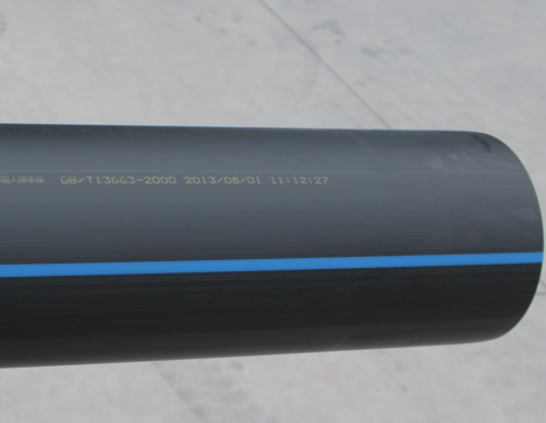
It can be used for bracelet processing, fly marking, large-format garment engraving, multi-scanner processing, die cutting, tube processing, etc.

Contact Us
Service Hotline
Email: Click Me
Telephone:010-64426993/95
Headquarter: #22 Building, #13 Mintai Road, Shunyi District, Beijing City, China,101300.
Main Factory: 4th Floor, #15 Building, #13 Mintai Road, Shunyi District, Beijing City, China,101300.
Suzhou JCZ Technology Co., Ltd.
Address: m3-103-2, microsystem Park, Suzhou science and Technology City, No. 2, Peiyuan Road, Huqiu District, Suzhou, Jiangsu
Guangdong JCZ Technology Co., Ltd.
Address: room 1002, No. 4, Songhu Zhigu R & D center, No. 1, renju Road, Liaobu Town, Dongguan City, Guangdong Province
Beijing JCZ Technology Co., Ltd. Wuhan Branch
Address: 1101, block B, building 1, modern service industry base, Huagong science and Technology Park, University Park Road, Jiangxia District, Wuhan, Hubei Province
Copyright © 2022 Beijing JCZ Technology Co., Ltd. 京ICP备18045191号-1


